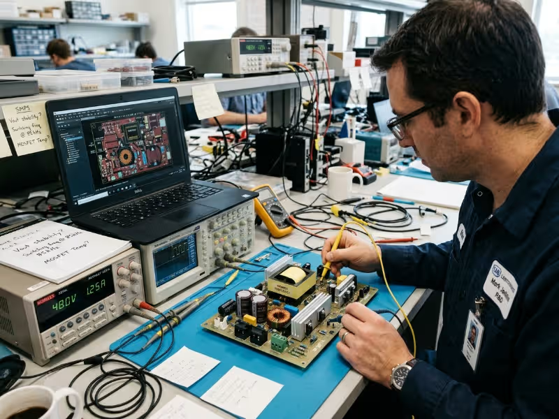
A switch-mode power supply (SMPS) does things a linear regulator simply can’t. It converts power at 85–95% efficiency instead of 30–60%, shrinks your magnetics and heat sinks, and holds a stable output across a 90–264 VAC universal input. Drop 12 V to 5 V at 2 A through a linear regulator and you burn 14 W as heat. A well-designed buck converter does the same job and wastes less than 1 W.
The decisions below are what separate a supply that passes certification and survives in the field from one that goes back to layout twice.
When to Consider Designing a Custom SMPS
The first real question isn’t how to design a supply — it’s whether you should design one at all. A custom SMPS pays off when volume, form factor, or performance targets rule out catalog modules. A pre-certified module ships in weeks and brings its safety approvals with it. A custom design takes months but wins on unit cost, fit, and control over every spec. Weigh these factors before you commit:
Application Volume and Type
Look at your annual volume before anything else. Engineering, safety certification, and EMC testing for a custom supply can easily run into six figures. If you ship 200,000 consumer chargers a year, saving $1.50 per unit returns $300,000 annually — custom design pays for itself fast. If you build 300 lab instruments a year, a certified module is almost always the smarter call.
Power Requirements
Write down every output rail with its voltage, continuous current, and peak current. Peaks matter more than most teams expect — a motor start or a radio burst can pull two to three times the average current for a few milliseconds. Then check total input power. Above 75 W input, IEC 61000-3-2 harmonic limits usually require power factor correction (PFC). If a 70 W design quietly grows to 80 W during development, you suddenly need an extra power stage that wasn’t in the budget.
Operating Environment
Check the full ambient temperature range, humidity, vibration, and airflow. Altitude matters too. Above 2,000 m, air breaks down at lower voltages, so clearance distances must increase — by roughly a factor of 1.48 at 5,000 m. If your enclosure is sealed and fanless, every watt of loss must escape through the walls. That means derating components and pushing the design toward higher efficiency from the start.
Efficiency Targets
Know which benchmarks your market requires before you pick a topology. External power supplies must meet DoE Level VI in the U.S. and EU CoC Tier 2 in Europe. PC and server supplies compete on 80 PLUS ratings. Think of efficiency as a product feature, not just a compliance checkbox. At 1 kW output, moving from 92% to 94% efficiency cuts losses from 87 W to 64 W — that’s roughly 25% less heat to manage.
Define Your Specifications and Budget
Component costs vary by region, supplier, and market conditions. Your biggest BOM cost drivers are usually GaN or SiC switches, custom magnetics, and safety-rated Y-capacitors. Lead times on custom transformers can stretch past 12 weeks. Confirm availability and second sources before you freeze the bill of materials.
Budget in cost per watt ($/W). If your product can carry a $6 supply at 60 W, your target is $0.10/W, and every part must justify its place. You can’t estimate cost accurately until you’ve locked these specs:
- Input voltage range
- Output voltage and current per rail
- Ripple and noise limit (mV peak-to-peak)
- Line and load regulation (%)
- Hold-up time (ms)
- Isolation rating
Each spec has a direct cost consequence. Tightening ripple from 100 mV to 20 mV adds a second LC filter stage and several low-ESR capacitors. Doubling hold-up time from 10 ms to 20 ms roughly doubles the energy in your bulk capacitor. Write specs from what the load actually needs — not from a template someone used on a different project.
Optional features raise cost fast. Digital control, PMBus telemetry, active PFC below the 75 W threshold, and N+1 redundancy each add parts, firmware, and test time. On a tight budget, ask one honest question about each feature: will the end customer notice if it’s gone? If not, cut it.
Determine Your Size, Space, and Thermal Limits
Measure the available space before you choose a single component. Record the PCB footprint, maximum component height, and enclosure volume. Height is often the binding constraint — the transformer and bulk capacitors are the tallest parts on the board, and a 12 mm height limit rules out many standard electrolytic capacitors and off-the-shelf bobbins.
Switching frequency determines how small those parts can be. Moving from 100 kHz toward 1 MHz shrinks the transformer and output capacitors significantly. GaN switches push practical designs into the several-MHz range. The trade-off is higher switching loss and harder EMI. Leave thermal headroom for heat sinks, copper pours, and airflow. Also reserve physical room for the input EMI filter, connectors, and test points — teams that skip this end up fighting for board space at the worst possible time.
Start layout with the largest, most constrained component, which is usually the transformer or main inductor. Size it for your power level and switching frequency, confirm it clears the height limit with margin, then arrange the switches, rectifiers, and bulk capacitors around it. This order keeps high-current paths short. If the magnetic part doesn’t fit, change the frequency or power level now — not after layout is 80% complete.
Think About Its Use Case
The end application sets your design priorities. Consumer electronics, industrial automation, medical devices, and automotive systems all use SMPS topologies, but they weight the same five parameters very differently:
- Efficiency: Lower losses reduce heat, shrink the enclosure, and cut lifetime energy cost.
- Reliability: MTBF targets and capacitor lifetime ratings at real operating temperatures determine how long the product survives.
- Power density: Watts per cubic inch decides whether the supply fits inside compact or sealed products.
- Cost: BOM pressure dominates high-volume markets where a few cents per unit multiplies into real money.
- EMC: Conducted and radiated emission limits determine whether your product can legally ship.
Industrial
Industrial supplies must survive harsh conditions for a decade or more. Expect wide input ranges, DIN-rail form factors, and operation from −40°C to +70°C. Surge immunity under IEC 61000-4-5 is non-negotiable, because factory lines carry motor and switching transients. Use capacitors rated for 105°C and long service life — a component that lasts 2,000 hours at 85°C may only survive 500 hours if the real operating temperature is 10°C higher.
Consumer Electronics
Consumer products compete hard on cost and size. A USB-C charger must deliver multiple USB Power Delivery voltage profiles — 5 V, 9 V, 15 V, and 20 V — from one compact flyback design. No-load standby power must stay below 0.1–0.3 W to satisfy efficiency rules. Every cent in the BOM matters when you ship millions of units, so topology selection, magnetics sourcing, and controller choice all carry real financial weight.
Telecommunications
Telecom equipment can’t go down. Most systems run from a −48 V DC bus that swings from −36 V to −72 V. Supplies need hot-swap capability so technicians can replace a module without shutting down the rack. Redundant operation and high-efficiency DC/DC brick converters are standard, because uptime and thermal density in packed racks drive every decision.
Medical
Medical supplies must protect the patient above all else. IEC 60601-1 requires 2 MOPP isolation for patient-connected equipment — that means 4,000 VAC withstand and 8 mm creepage minimum. Leakage current limits are strict and directly size your Y-capacitors. Low EMI matters too, because instruments like ECG monitors pick up switching noise. If you’re sourcing rather than designing, Quankang’s medical power supply range covers 5 W to 500 W with IEC 60601-1 certification and leakage current held to ≤100 µA across the full input range.
Automotive
Automotive power faces the harshest electrical environment in this list. You may design for a 12 V, 48 V, or high-voltage EV bus. Load dump and transient tests under ISO 7637-2 and ISO 16750 can hit your input with spikes well above nominal. ICs must be AEC-Q100 qualified and passives AEC-Q200 qualified. Emissions must meet CISPR 25, which is stricter than most consumer limits and applies across a wide frequency range.
Consider Your Load Requirements
Knowing the load matters as much as knowing the input. Many supplies pass bench tests on an electronic load and then fail with the real product. Before you finalize the design, profile the load: is it steady or pulsed? Resistive, capacitive, or inductive? How sensitive is it to noise? A large capacitive load can trip overcurrent protection at startup. An inductive load can push energy back into the output. A well-specified SMPS holds regulation from no load to full load and through every transient in between.
Here is how requirements shift across load classes:
- Low-power loads (under 10 W): Microcontrollers, sensors, and IoT nodes spend most of their life in sleep modes. Light-load efficiency matters far more than peak efficiency. Choose controllers with burst-mode operation and low quiescent current — often under 10 µA — to extend battery runtime from months to years.
- Mid-power loads (10–200 W): Laptops, LED drivers, and networking gear need balance. Efficiency, cost, and transient response all matter, and none can dominate. LED drivers also add a constant-current requirement and flicker limits, so check the load’s own standards early in the project.
- High-power loads (200 W and above): Servers, motor drives, and EV chargers make thermal management the central design problem. PFC is required by regulation, and many designs parallel multiple converter units. Paralleled supplies need active current sharing — without it, one unit carries most of the load and fails first.
- Dynamic and pulsed loads: CPUs, RF amplifiers, and motors step their current demand in microseconds. These loads demand high loop bandwidth, low-ESR output capacitance, and a phase margin of at least 45°. Below that margin, the output rings after every load step, and the downstream circuit may reset or malfunction.
Choose Your Design Architecture
Decide on isolation before you pick a topology. Mains-connected and safety-critical outputs need galvanic isolation through a transformer so that a primary-side fault can never reach the user or patient. Point-of-load rails on a board that is already isolated can use smaller, simpler non-isolated converters. A common and effective approach uses both: one isolated stage creates a 12 V or 48 V intermediate bus, then a set of non-isolated converters step it down to each point-of-load rail. Match the architecture to the safety class and the load — not to what was used on the last project.
Then match the control scheme to the system:
- Peak current-mode control is easier to compensate and gives built-in cycle-by-cycle current limiting.
- Voltage-mode control is less sensitive to noise, which helps in noisy layouts or at very light loads.
- Digital control adds telemetry, reconfigurability, and fault logging.
If you build a product family, standardize on one controller IC family and one feedback approach. Shared parts simplify qualification, reduce sourcing risk, and make cross-product debugging much faster.
Create an Efficient PCB Layout
A good schematic can still fail in layout. Start with current flow. Every converter has a hot loop — the high di/dt path through the input capacitor and power switches. Loop area drives radiated EMI and sets the peak voltage spike across the switch. Keep the input ceramic capacitor within a few millimeters of the switch and close that loop on a single layer when possible.
Next, separate noisy zones from quiet ones. The switch node swings hundreds of volts in nanoseconds and couples into anything nearby. Keep the feedback divider, compensation network, and current-sense traces well away from it. Use Kelvin connections for current sensing so the sense signal is free of power-path voltage drops. Route the feedback trace over an unbroken ground plane — a single slot under that trace is enough to inject noise that causes output jitter.
Finally, plan for heat and testability. Spread hot components apart and place thermal vias under power pads to move heat into inner copper layers. Add test points for the switch node, output ripple, and loop-response injection. Without them you can’t measure what the circuit is doing, and finding the root cause of a failure becomes guesswork.
Types of SMPS Topologies to Consider
With your specs, load profile, and architecture defined, the topology choice becomes much more straightforward. Picking the wrong one early costs more than any optimization can recover later.
Flyback Converter
The flyback stores energy in a coupled inductor during the switch on-time and delivers it to the output during the off-time. It is the most common choice for low-power AC/DC supplies because it needs no output inductor and handles multiple outputs easily.
- Best fit: Up to about 100–150 W, including multi-output supplies.
- Strengths: Lowest part count and lowest cost of any isolated topology.
- Trade-offs: High peak currents and leakage-inductance spikes on the primary switch at every turn-off.
- Design tip: Add an RCD clamp or active clamp to protect the MOSFET. An active clamp also recovers leakage energy and improves efficiency.
Forward Converter
The forward converter transfers energy through the transformer during the on-time rather than storing it, which gives it lower peak currents and better transformer utilization than a flyback.
- Best fit: About 100–500 W.
- Strengths: Lower output ripple and more efficient use of the transformer core.
- Trade-offs: Requires an output inductor and a core-reset mechanism each cycle.
- Design tip: An active clamp reset recycles magnetizing energy and allows duty cycles above 50%, which widens the usable input range considerably.
Buck and Boost Converters
Buck and boost converters are the non-isolated building blocks of most power systems. The buck steps voltage down at point-of-load; the boost forms the front end of most PFC stages.
- Best fit: Board-level rails and battery-powered products.
- Strengths: With synchronous rectification, efficiency often reaches 95% or higher in a compact footprint.
- Trade-offs: No isolation. A buck only steps down and a boost only steps up.
- Design tip: Use a buck-boost when the input voltage crosses the output voltage during operation — a single lithium cell feeding a 3.3 V rail is a classic example.
Full-Bridge Converter
The full-bridge drives a transformer in both directions using four switches, which gives the best core utilization and makes it the standard choice at high power.
- Best fit: 500 W to several kilowatts — servers, telecom rectifiers, and EV chargers.
- Strengths: Phase-shifted control achieves zero-voltage switching (ZVS), which cuts switching loss significantly at high power.
- Trade-offs: Highest complexity of the four topologies, with four gate drivers and demanding control design.
- Design tip: Consider an LLC resonant stage for fixed-ratio, high-efficiency DC/DC conversion after a PFC front end.
Safety and Compliance Considerations
Compliance is the final gate, and it’s not forgiving. A design that fails certification goes back to layout — sometimes months back. The engineers who plan for safety requirements from day one rarely face that outcome.
Most Common Safety Risks
Know these failure modes before you finalize the schematic:
- Electric shock from insufficient creepage or clearance across the isolation barrier
- Overheating or fire from overloaded components or a failed MOSFET
- Electrolytic capacitor wear-out at elevated temperature — capacitor lifetime roughly halves for every 10°C rise above the rated operating point
- EMI failures that block market approval and delay launch
How to Minimize Safety Risks
Build protection directly into the design. Include overcurrent, overvoltage, and overtemperature shutdown, plus inrush limiting and an input fuse. Size creepage and clearance distances to IEC 62368-1 for IT and consumer equipment, or to IEC 60601-1 for medical products. Mark those distances on the PCB layout from the very first revision — not after the first failed test report.
Validate before you commit to production tooling:
- Run hipot tests — around 3,000 VAC for reinforced insulation, depending on the applicable standard.
- Do thermal imaging at full load and maximum ambient temperature.
- Run pre-compliance EMI scans against CISPR 32, or CISPR 11 for industrial and medical equipment.
Repeat these checks after every significant layout change. A small copper pour modification can shift a hot spot or crack open an emissions problem that wasn’t there in the previous revision.
Ready to Move From Design to Production?
If your SMPS design is headed toward certification and volume manufacturing, the supplier you choose for the power stage matters as much as the topology you pick. Quankang has been designing and manufacturing certified AC-DC power supplies for 36 years, with an in-house EMC lab that runs pre-compliance testing to FCC and CE standards before anything reaches a third-party certification body. That alone typically saves four to six weeks per project. Their range covers medical-grade supplies built to IEC 60601-1, USB PD chargers from 20 W to 240 W, and custom power adapter programs for ODMs with specific form factor or output requirements. If you have a spec in hand, their engineering team responds within 24 hours.