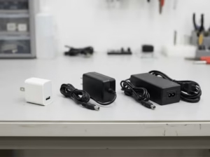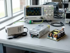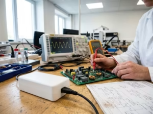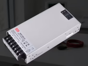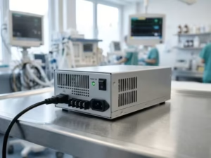
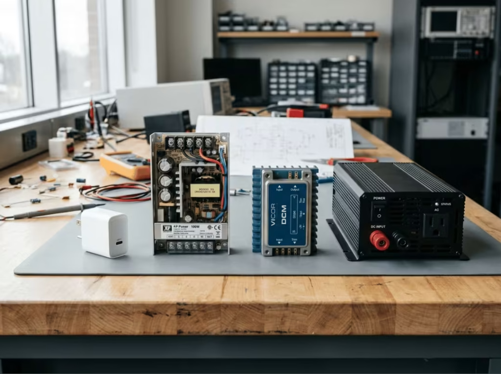
Your phone charger, laptop adapter, and EV charging station all do the same thing: reshape electrical energy into a form the load can actually use. The topology behind that conversion—flyback in a 65 W adapter, full-bridge in a solar inverter—determines how much heat you manage, how long the product lasts, and whether it clears compliance testing.
This guide focuses on the decisions that matter: when to use a linear regulator instead of a switcher, which converter topology fits your power level and isolation requirement, why efficiency and thermal design are the same problem, and why a design that passes simulation can still fail on the bench. The goal isn’t to survey every power electronics equation—it’s to give you a repeatable way to match a converter to a real project.
What Power Conversion Actually Involves
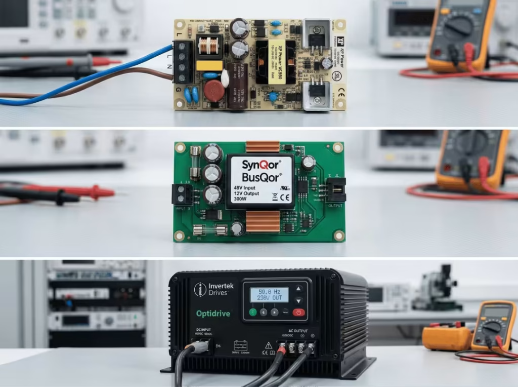
Power conversion means delivering electrical energy in exactly the form a load requires—the right voltage, current, and waveshape. Every practical conversion falls into one of four categories.
AC-to-DC (rectification) is what happens inside every charger and server power supply. It’s the most common conversion in electronics, and the one most engineers optimize hardest.
DC-to-DC converts one DC voltage to another—stepping down a battery pack to feed a 1.8 V processor rail, or boosting a single cell to drive an LED string. Most PCBs contain several DC-DC stages, often more than the schematic makes obvious.
DC to AC (inversion) synthesizes an AC waveform from a DC source. Solar inverters, UPS systems, and motor drives all work this way.
AC-to-AC changes voltage or frequency directly and is important in specific industrial drives, but it’s uncommon enough that this guide sets it aside.
Identifying which conversion you need is the first real design decision. It immediately constrains topology options and determines whether isolation belongs in scope.
Why Conversion Efficiency Is Never Just a Spec
Energy conservation is non-negotiable: output power can never exceed input power, and the difference is dissipated as heat. That single fact ties efficiency, thermal design, and component lifetime into one chain.
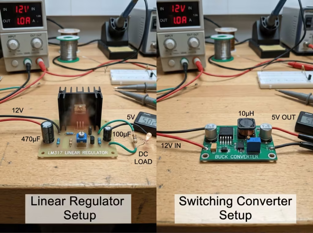
A concrete example clarifies this. To get 5 V at 1 A from a 12 V source, a linear regulator drops 7 V across its pass transistor while passing 1 A—that’s 7 W dissipated to deliver 5 W, roughly 42% efficiency. A well-designed buck converter doing the same job reaches 90% or better, wasting under a watt.
Seven watts in a confined package is a real engineering problem. It demands a heatsink, heavy copper pours, or forced airflow to stay within safe limits. Temperature degrades everything: electrolytic capacitors lose roughly half their rated lifetime for every 10 °C rise, semiconductors derate, magnetics saturate more easily at high temperatures, and solder joints fatigue under thermal cycling.
Moving from 42% to 90% efficiency doesn’t just cut the electricity bill. It reduces heatsink size, extends component life, and often lowers total system cost. Efficiency is a system-level concern—not a checkbox—and the linear-versus-switching decision is usually where most of it is won or lost.
Linear or Switching? Making the First Decision
Before picking a topology, you pick a strategy. Linear regulators and switching converters solve the same problem in fundamentally different ways. Getting this decision right early prevents a lot of rework downstream.
When a Linear Regulator Is the Right Answer
A linear regulator places a transistor in series with the load and uses it to drop the excess voltage. The output remains regulated, but efficiency is directly capped by the voltage ratio V_out/V_in.
That limitation doesn’t disqualify it. LDOs are quiet—they generate none of the high-frequency switching noise that plagues sensitive analog and RF rails. They need minimal external components, typically just two capacitors. And when the voltage drop is small, or the current is low, the inefficiency barely matters. A regulator dropping 3.3 V to 3.0 V at 50 mA wastes 15 mW—a non-issue. For precision references, ADC supply rails, always-on housekeeping supplies, and the post-regulation stage of a hybrid supply, an LDO is often the correct choice even when a switcher would score better on an efficiency chart.
Why Switching Converters Dominate at Medium and High Power
A switching converter doesn’t dissipate the excess—it routes energy through an inductor and capacitor using a high-frequency switch, transferring only what the load actually needs. Pulse width modulation (PWM) controls how much energy moves each cycle. Because the switch is ideally either fully on or fully off, losses are far smaller than in a linear pass element. That’s how switchers reach 85–95% efficiency across large voltage differences and high currents.
The trade-off is real: fast-switching edges generate EMI; the design requires careful board layout; and you’re now managing an inductor, a control loop, and switching noise. None of it is insurmountable, but it’s engineering work that an LDO simply doesn’t ask for.
Five Questions That Settle the Choice
Rather than applying rules of thumb, ask these directly about your rail:
- How large is the voltage gap? A big gap destroys linear efficiency.
- How much current does the load draw? High current amplifies any voltage drop into serious heat.
- How tight is the noise budget? Sensitive analog and RF loads often demand a linear stage.
- How constrained are board area and thermal headroom? Both arguments push against wasted power.
- Which matters more—simplicity or efficiency? On a 20 mA housekeeping rail, an LDO is often the better engineering call.
A 12 V-to-1.2 V rail at 3 A belongs in switching territory, full stop. A 5 V to 3.3 V rail at 20 mA feeding a precision reference belongs to an LDO.
The Hybrid Pattern Most Production Designs Use
The two aren’t mutually exclusive. A common approach uses a switching pre-regulator for the heavy voltage reduction, followed by an LDO to clean up ripple and noise for a sensitive load. You capture most of the switcher’s efficiency and most of the LDO’s quiet. This appears constantly in RF front-ends, high-resolution data acquisition, and precision analog designs where both efficiency and noise floor matter.
DC-DC and AC-DC Converter Topologies: Which One Fits Your Design
Committing to switching narrows the field but doesn’t finish the choice. Five or six topologies cover the overwhelming majority of real designs. The right question about each isn’t “how does the math work?”—it’s “what problem does this solve, and what does it cost me?”
Buck Converters: The Default for Stepping Down Voltage
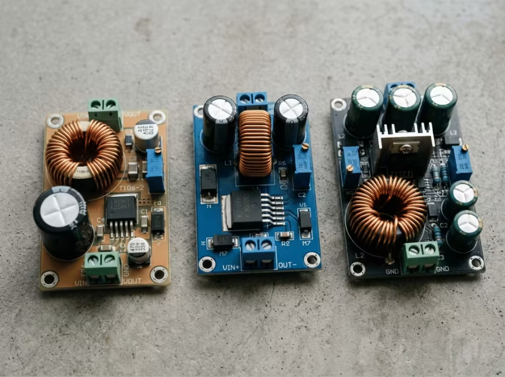
The buck converter is the most common topology in electronics. It steps a higher DC voltage down to a lower one, with output voltage governed by duty cycle: V_out ≈ D × V_in. At 25% duty cycle on a 12 V input, the output is roughly 3 V. The relationship is linear and easy to control.
Bucks appear everywhere—CPU core rails, GPU supplies, memory rails, and point-of-load regulators across industrial electronics—because they’re well understood, well supported by integrated controllers, and highly efficient. Design effort goes into managing output ripple, quickly handling load transients, and keeping the high-current switching loop tight on the board. Get those three things right, and a buck is a largely solved problem.
Boost Converters: When Your Input Voltage Is Too Low
When the output needs to be higher than the input, the boost converter steps up. It stores energy in an inductor during the switch on-time, then releases it in series with the input when the switch opens—producing a higher output. Single-cell battery systems rely on boost stages to power circuitry requiring 3.3 V or 5 V from a cell that may sag below 3 V at end of life.
The trade-off: input current is continuous and can be high, since all load energy must flow through the lower-voltage source. Switch and diode voltage stress rises with the output level. The control loop also contains a right-half-plane zero that limits response speed—a real constraint that needs explicit attention during compensation.
Buck-Boost and SEPIC: For Wide or Unpredictable Input Ranges
Not every source stays conveniently above or below the target. A lithium-ion cell swings from about 4.2 V fully charged to 3.0 V depleted, which brackets a common 3.3 V target—requiring both step-down and step-up capability depending on state of charge. Automotive electronics face a similar challenge, where the nominal 12 V rail sags below 6 V during cold cranking and spikes well above nominal during load dump.
Buck-boost and SEPIC topologies handle this by converting in either direction as needed. The cost is complexity: more components, somewhat lower efficiency, and higher switch stress compared to a pure buck or boost. Choose them when the input range genuinely demands it—not as a default.
Isolation: When Ground Sharing Isn’t an Option
Every topology above shares a common ground between input and output. Sometimes that’s not permitted. Safety regulations require galvanic isolation between the AC line and anything a user can touch. Isolation also breaks ground loops in systems with multiple power domains and makes very large voltage ratios practical without extreme duty cycles. When isolation is required, you move from inductor-based topologies to transformer-based ones. The transformer now provides the conversion pathway and the safety barrier simultaneously, and the design changes in character.
Flyback Converters: Why They Appear in Almost Every Small AC-DC Supply
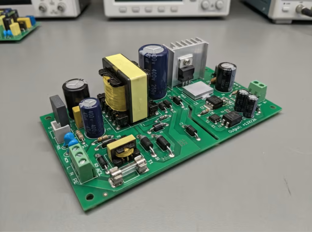
Below roughly 100 W, the flyback converter is the dominant isolated off-line topology. Open a phone charger, a 45 W laptop brick, or a small ITE power supply, and you’ll almost certainly find one. Its appeal lies in architectural simplicity: a single coupled inductor serves simultaneously as a storage element and a transformer, providing isolation, voltage transformation, and regulation with a minimal switch count. Energy is stored in the transformer core during the switch-on time and transferred to the output when the switch turns off.
That simplicity is also the flyback’s ceiling. As power increases, peak transformer currents rise steeply, switch-voltage stress increases, output ripple becomes harder to filter, and EMI worsens. The flyback is the right answer at low power and progressively worse beyond 75–100 W.
Higher-Power Isolated Topologies: Forward, Half-Bridge, and Full-Bridge
Above the flyback’s comfortable range, the design logic shifts to topologies that transfer energy through the transformer while the switch is on—rather than storing it in the core. The forward converter is a common next step at mid power. Push further, and half-bridge or full-bridge topologies drive the transformer in both directions, improving core utilization and reducing per-switch stress—at the cost of more switches and more complex gate-drive circuitry.
The pattern is consistent: as power climbs, designers accept greater control and drive complexity in exchange for improved efficiency and reduced component stress.
A Five-Question Topology Selection Framework
When facing a blank schematic, five questions get you to a short list quickly:
- AC or DC input? AC input means rectifying first and almost always means isolation.
- Is isolation required? Yes, points directly to a flyback, forward, or bridge topology.
- What is the power level? The strongest single driver—flyback up to roughly 100 W, forward and bridge topologies beyond.
- How wide is the input voltage range? Wide ranges on the non-isolated side favor a buck-boost or SEPIC topology.
- What is the binding constraint—efficiency, noise, size, or cost? This breaks ties when multiple topologies are viable.
Treat the power boundaries as engineering guidance, not hard rules. GaN and SiC devices keep shifting, with each topology being practical in different cases. Use the framework to identify two or three candidates, then validate them against current reference designs before committing.
Efficiency, Losses, and Thermal Limits
Choosing the right topology still leaves a design that can run hot and fail prematurely if you don’t track where losses originate. Efficiency is the net result of four distinct mechanisms, and you have some control over each.
The Four Loss Sources Every Designer Should Know
Conduction losses are I²R losses in the switch, the output rectifier, and the inductor or transformer windings. They dominate at high load and scale with the square of the current—doubling the current quadruples the conduction loss. Lower on-resistance switches, synchronous rectifiers, and optimized winding resistance all reduce this.
Switching losses occur at every on-to-off and off-to-on transition, when the switch briefly carries significant voltage and current simultaneously. The energy lost per transition is roughly fixed, so total switching loss scales directly with frequency.
Core losses—hysteresis and eddy currents in the inductor or transformer—grow with both switching frequency and flux swing. Core material selection matters more than many designers appreciate.
Fixed losses, including gate drive power, control IC consumption, and bias supplies, are small at full load but dominate at light load. They largely set standby power consumption and light-load efficiency, which matters more than expected for products that spend most of their time idling.
Why You Can’t Just Raise the Switching Frequency
Higher switching frequency enables smaller magnetics and capacitors, which reduce board size. The problem is that switching and core losses both increase with frequency, generating heat and EMI. For a given semiconductor technology, there is a frequency that minimizes total loss; beyond it, you’re trading efficiency for size with no net benefit. Switching frequency is one of the earliest decisions to lock in because it drives magnetics sizing, the loss budget, and EMI behavior throughout the entire design.
Thermal Analysis Belongs at the Start, Not the End
Heat generated inside a converter travels through a series of thermal resistances—junction to case, case to heatsink or PCB copper, and then to ambient air. These resistances add in series, and the total determines how hot the junction runs at a given dissipation level.
The consequence is that continuous power capability depends on cooling conditions, not just on silicon ratings. A power FET that handles 50 W with a heatsink and forced airflow might be reliable at only 5 W soldered to a small board with no airflow. Estimating junction temperature from the datasheet’s thermal resistance figures and expected dissipation should happen early in the design—not as a retrospective check when the board runs too hot.
How Losses Tie Directly to Reliability
Reducing losses not only improves efficiency—but it also extends the product’s working life. Electrolytic capacitors, the most common failure point in power supplies, lose roughly half their rated service life for every 10 °C rise in operating temperature. Semiconductors, transformer insulation, and solder joints all degrade faster under thermal stress. Every watt of dissipation you eliminate is a thermal problem that never needs to be solved, and every degree you keep off the capacitors adds time to the product’s field life.
Why Designs That Simulate Well Still Fail on the Bench
Some of the most expensive power supply failures involve designs that were thoroughly simulated and looked correct on paper. The gap between a working schematic and working hardware almost always traces to three areas that simulators don’t model well.
Control Loop Stability Is Harder Than It Looks
A switching converter holds its output steady through a feedback loop: sense the output, compare it to a reference, and adjust duty cycle to correct the error. That loop has a gain and a phase response. If the gain is too high where the phase approaches 180°, the loop oscillates. If compensation is insufficient, the output rings and hunts rather than settling.
Load transients expose this clearly. When a processor jumps from idle to full load in microseconds, the control loop must respond quickly enough to keep the output within tolerance. A well-compensated converter recovers quickly with a small voltage dip. A poorly tuned one sags, overshoots, and rings before settling. The compensation math is well established, but it requires verification on actual hardware—ideal component models in simulation don’t capture the real behavior of the error amplifier and feedback network at the operating point.
Switching Edges Generate EMI That Filtering Alone Can’t Solve
The fast voltage and current transitions that make switching converters efficient also make them noisy. A switching node that moves from 0 V to 48 V in 10 ns generates high-frequency energy that couples into input and output wiring as conducted EMI and radiates from layout loops. Regulatory standards—CISPR 32, FCC Part 15, and their equivalents—set hard limits on both.
The common mistake is treating EMI as a compliance step at the end: add a filter and hope. Filters attenuate noise after the fact, but if the source is strong—a large switching loop, a long gate-drive trace, high interwinding transformer capacitance—the filter may lack sufficient headroom to bring emissions below the limit without becoming unreasonably large. Effective EMI mitigation starts with minimizing the source. The filter handles what’s left.
Board Layout Is Part of the Circuit Design
Layout is where many converter failures originate, and it’s the area where even experienced designers tend to underestimate the impact. The high-frequency current loop between the input capacitor, power switch, and inductor is an antenna. The larger the loop area, the stronger the radiation and the more parasitic inductance in the path—which causes voltage ringing at the switch node, stressing the device and worsening EMI.
Rules that consistently matter: place the input decoupling capacitor as close to the switch as possible with a direct copper path. Keep gate drive traces short. Use a solid ground plane under the controller. Place the controller close to the switch so that current-sense and feedback paths remain short. These aren’t preferences—the same schematic can pass or fail EMI compliance based purely on layout, and this plays out repeatedly in real lab environments.
How to Choose the Right Power Converter for Your Application
All of this converges on one practical question: given your actual requirements, what do you build? The process is straightforward when worked through in the right order.
Define the Specification Before Looking at Parts
Before reviewing any datasheet, nail down what the design actually needs. Define the full input voltage range—not nominal, but worst-case low and high, including transients. Set output voltage and peak current. Decide whether isolation is required. Specify output ripple limits and the transient response the load demands. Add the efficiency target, operating temperature range, board area constraint, and cost target.
These numbers drive every subsequent decision. Skipping them is how projects end up selecting topologies that are theoretically viable but wrong for the application—and then spending multiple board spins to correct them.
Three Scenarios That Illustrate the Selection Logic
A 12 V to 5 V board-level rail. At 200 mA, an LDO dissipates 1.4 W—often manageable, and the design is trivially simple. At 1 A, that LDO dissipates 7 W and requires proper thermal management. An integrated buck at 1 A wastes under a watt and fits in a smaller footprint than the LDO plus heatsink. The decision is current magnitude and board thermal budget, not topology preference.
A 65 W USB-C charger. Off-line, isolated, compact. The topology is almost always a flyback or active-clamp flyback with synchronous rectification. Active-clamp flyback recycles leakage-inductance energy rather than dumping it into a snubber, which meaningfully improves efficiency at this power level. Design priorities: full-range efficiency, low standby power, safety compliance, and thermal management within a small enclosure. For a closer look at how these design priorities play out in finished products, the USB PD Chargers page illustrates what this topology enables at the product level.
A 3 kW solar inverter. DC from the panels must be converted to grid-quality AC. A typical architecture first boosts and stabilizes the DC bus, then a full-bridge or multilevel inverter synthesizes the AC waveform using sinusoidal PWM. The control system tracks grid frequency and phase in real time, holds total harmonic distortion below regulatory limits, and handles faults cleanly. Thermal management is a first-class design concern because currents are large and operation is continuous.
A Repeatable Decision Path
The same logic applies across projects. Is the input AC? Rectify first, plan for isolation, check PFC requirements. Is isolation mandatory? Go transformer-based. What is the power level? That selects among flyback, forward, and bridge. How wide is the input range? That resolves the non-isolated topology question. What is the tightest constraint—efficiency, noise, size, or cost? That breaks remaining ties.
Work through those questions in that order, and the topology choice usually becomes clear without evaluating every option from scratch.
Common Mistakes Worth Knowing About
A few misconceptions recur and tend to surface late in projects, when they’re expensive to fix.
A larger inductor is always better. Oversizing the inductor reduces ripple current but slows the transient response, increases winding resistance, costs more, and takes up more board space. More critically, specifying an inductor without verifying its saturation current rating means the core can saturate under peak load, losing most of its inductance exactly when you need it most.
Peak efficiency is what matters. A converter that’s 95% efficient at full load might drop to 75% at 10% load. If the product spends most of its life at light load—which many do—the headline number is misleading. Efficiency curves across the full load range tell the real story, and well-made datasheets show them.
A 100 W rated converter delivers 100 W continuously. Not without the thermal environment the rating assumes. In a sealed enclosure with no airflow, the same converter will overheat, derate, or fail. Rated power reflects cooling conditions, not just silicon capability.
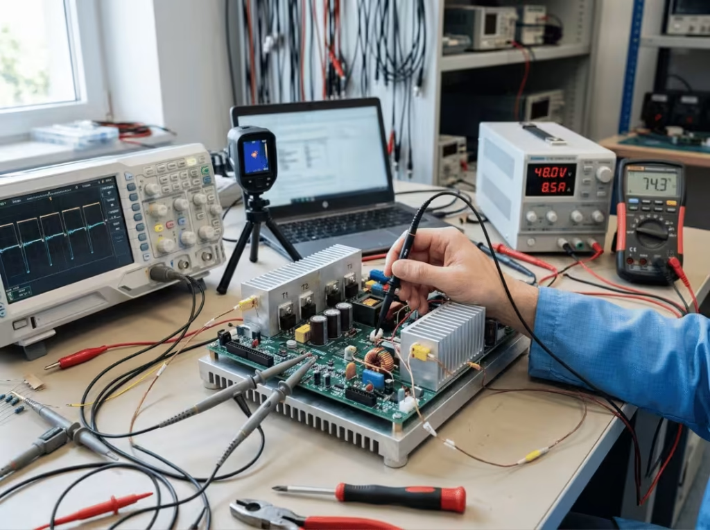
Simulation success guarantees bench success. Simulators use ideal switches, ideal layout, and ideal component values. Real hardware has parasitic inductance in traces and vias, component tolerances that stack across a design, temperature coefficients that shift behavior over the operating range, and a switching node that radiates energy in ways SPICE doesn’t capture. Build it, probe it, and measure what matters.
Frequently Asked Questions
What is the difference between a linear regulator and a switching regulator?
A linear regulator drops the excess voltage across a pass transistor, converting the difference directly into heat—simple and quiet, but inefficient for large voltage drops or high currents. A switching regulator cycles a switch to transfer only the energy the load needs, reaching much higher efficiency at the cost of switching noise and a more complex design.
What is the difference between isolated and non-isolated converters?
An isolated converter uses a transformer to provide galvanic separation between the input and output, which is required for safety on AC-line-powered equipment and is also useful for breaking ground loops. A non-isolated converter shares a common ground, is simpler to design, and is typically more efficient—making it the standard choice for board-level DC-DC rails.
What is duty cycle and how does it affect output voltage?
Duty cycle is the fraction of each switching period that the main switch is on. In a buck converter, the output voltage is approximately the input voltage multiplied by the duty cycle: a 25% duty cycle on a 12 V input produces roughly 3 V. The control loop adjusts the duty cycle continuously to hold the output at the target.
Why does a buck converter need an inductor?
The inductor stores energy while the switch is on and releases it while the switch is off, smoothing the pulsed current into a steady DC output. Without it, the load sees raw switching pulses with no filtering mechanism. The inductor isn’t a passive filter added afterward—it is the conversion mechanism itself.
Why does switching frequency matter so much?
Higher frequency enables smaller magnetics and capacitors, shrinking the design. But switching losses and core losses both increase with frequency, raising heat and EMI. The right frequency balances component size against efficiency and thermal constraints—it should be chosen intentionally, not pushed to the maximum the controller allows.
Why is power factor correction used in AC-DC supplies?
Without correction, the bulk capacitor draws current in narrow spikes around the voltage peaks, creating high harmonic content and a poor power factor. PFC forces the input current to follow the voltage waveform, raising the power factor to close to 1.0 and reducing harmonic distortion. Most markets require it in off-line supplies above roughly 75 W, though exact thresholds vary by region.
Conclusion
Every power conversion decision follows the same chain: identify the input-output relationship, decide whether isolation is required, match the topology to the power level, and set efficiency and thermal targets tight enough to keep the design reliable over its working life. Those four steps, taken in that order, resolve most topology choices without needing to evaluate every option.
What separates functional designs from robust ones isn’t knowing more topologies—it’s knowing which questions to ask before picking parts. Start from a clearly written specification, use established reference designs as a starting point rather than a finished answer, and measure what matters on real hardware: efficiency across the load range, output ripple and transient response, component temperatures, and emissions. If you’re curious about how these principles translate into manufacturing capabilities and test processes, the Facilities page offers a concrete look at what production-ready power conversion development entails. The loop between building and measuring is where power conversion judgment actually develops—and where reliable designs get made.