A 300mm silicon wafer sits inside a plasma etch chamber. For the next few minutes, it has to stay perfectly flat and still while it sheds heat into the surface beneath it. Nothing can touch its front side, because that’s where the circuits are being formed.
Suction can’t hold it in place, either. The chamber is under vacuum, so there’s no air pressure to create a holding force. The answer is electrostatic clamping, and the part that makes it work is the electrostatic chuck (ESC) power supply.
This guide explains how an ESC power supply creates clamping force and what it controls during a process run. It also covers how the wafer gets released cleanly and which specifications to check when you evaluate or specify a unit.
What Does an ESC Power Supply Do?
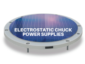
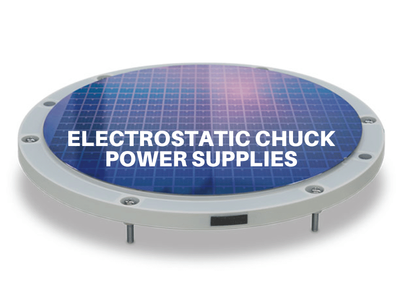
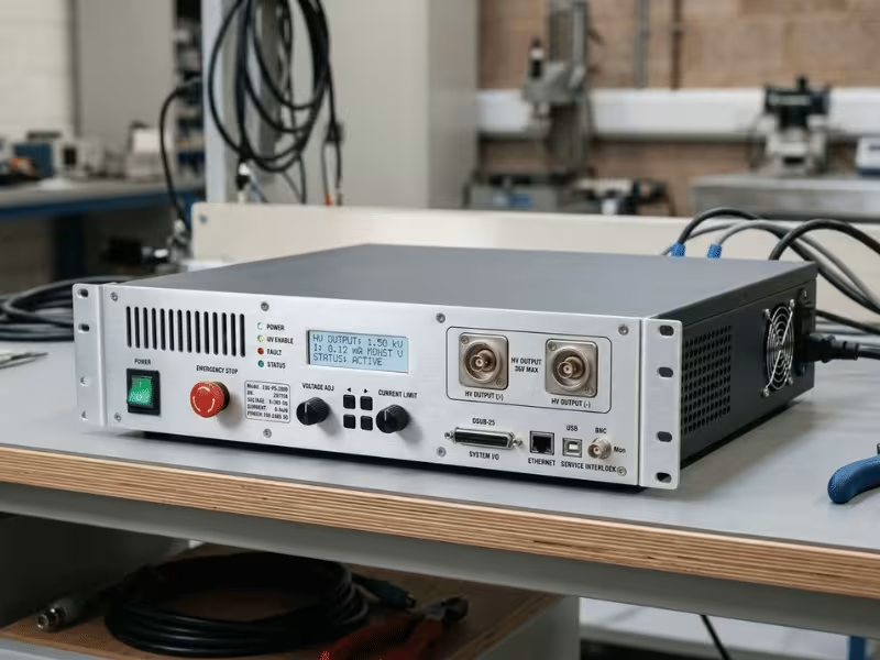
An electrostatic chuck power supply is a precision high-voltage DC source. It charges electrodes embedded inside the chuck, which is the platform the wafer rests on. That charge creates an electric field strong enough to hold the wafer against the chuck surface.
It helps to separate the two roles clearly. The chuck is the hardware that physically supports the wafer. The power supply controls the force: how much is applied, how quickly it builds, how steady it stays, and how cleanly it’s removed.
Think of it this way: if the chuck is the hand, the power supply decides how hard it grips and when it lets go. A good grip with a clumsy release still breaks wafers. That’s why the supply matters as much as the chuck itself.
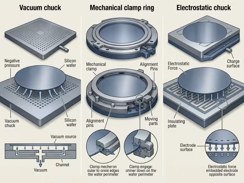
Why Not Use Vacuum or Mechanical Clamps?
High voltage might seem like a complicated way to hold a thin disc in place. But the simpler options run into real limits inside process chambers.
Method | How It Holds the Wafer | Limitation in Process Chambers |
|---|---|---|
Vacuum chuck | Pressure difference between the front and back of the wafer | Doesn’t work when the chamber itself is under vacuum |
Mechanical clamp ring | Physical ring pressing on the wafer edge | Generates particles, blocks usable edge area, and can cause uneven thermal contact or wafer bow |
Electrostatic chuck | Electric field attracts the wafer across its back surface | Needs a controlled high-voltage supply and careful release (dechuck) management |
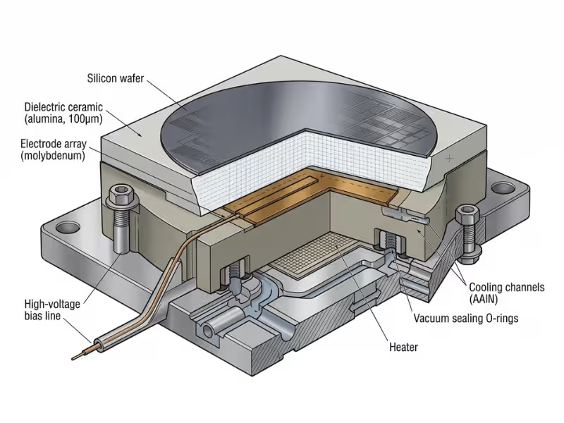
An ESC spreads the clamping force across the entire back of the wafer, with no front-side contact. That even contact also creates a good seal for helium backside cooling, where a thin layer of helium gas carries heat from the wafer into the temperature-controlled chuck. For processes where temperature affects results, that thermal path is often as important as the holding force itself.
How an ESC Power Supply Creates Clamping Force
The simplest way to picture an electrostatic chuck is as a parallel-plate capacitor. The electrode inside the chuck is one plate. The wafer is the other plate. A thin dielectric (insulating) layer sits between them.
When the power supply applies voltage to the electrode, opposite charges build up on either side of the dielectric. Opposite charges attract, so the wafer is pulled flat against the chuck surface.
Two factors shape how strong that pull is. Clamping force rises sharply with applied voltage, roughly with its square in the classic capacitor model. It falls off quickly as the dielectric gets thicker or the gap between wafer and chuck grows. That’s why surface flatness, cleanliness, and wafer bow all affect clamping, even when the supply output is perfectly stable.
Coulomb vs. Johnsen-Rahbek Chucks
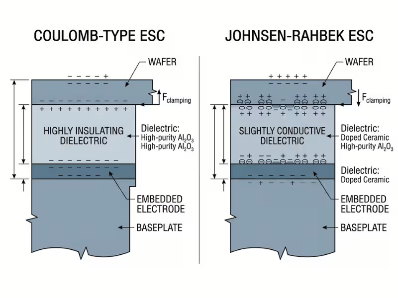
Not every ESC behaves the same way electrically. The dielectric material determines which of two clamping mechanisms dominates, and that changes what the power supply has to deliver.
Coulomb-type chucks use a highly insulating dielectric. The clamping force comes almost entirely from the capacitive field described above. Because the dielectric blocks current so effectively, these chucks typically need higher voltages, often in the low-kilovolt range, while drawing very little leakage current.
Johnsen-Rahbek (J-R) chucks use a slightly conductive dielectric, such as certain doped ceramics. A small current flows through the material, and charge collects at the microscopic gap between the chuck surface and the wafer. Because that gap is so small, J-R chucks can produce strong clamping force at noticeably lower voltages than Coulomb designs.
That advantage comes with a trade-off for the power supply. A J-R chuck draws continuous leakage current, and that current often changes with temperature. The supply has to deliver that current stably, monitor it, and limit it safely if something goes wrong.
The practical lesson is simple. Voltage range and current limits should come from the chuck manufacturer’s datasheet, not from a general rule of thumb. Two chucks that look similar can need very different supplies.
Monopolar vs. Bipolar: Why Chuck Design Changes the Supply
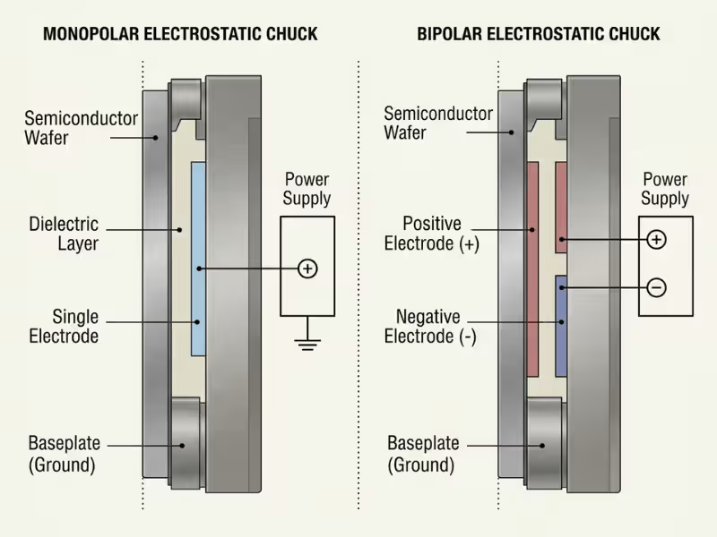
The second big design choice is how many electrodes the chuck uses and how they’re powered.
In a monopolar chuck, a single electrode is biased relative to ground. To clamp fully, the wafer usually needs an electrical return path, which is often provided by the plasma in the chamber. The design is simpler, but clamping depends on plasma being present.
In a bipolar chuck, two electrodes carry opposite polarities, such as +V and −V. The field forms between the electrodes and the wafer without needing plasma as a return path. That makes bipolar chucks useful for steps where no plasma is running, such as wafer transfer or certain non-plasma processes.
Attribute | Monopolar | Bipolar |
|---|---|---|
Electrode setup | One electrode, biased relative to ground | Two electrodes at opposite polarities |
Plasma needed to clamp fully | Usually yes | No |
Supply output | Single high-voltage output | Dual or bipolar output, typically balanced |
Typical use | Plasma-based processes with simpler chuck designs | Processes needing clamping without plasma, or more independent control |
The takeaway: a supply built for a monopolar chuck can’t simply be swapped onto a bipolar one. Output configuration, polarity handling, and balance between outputs all need to match the chuck design.
One Wafer, Start to Finish: The Chuck–Process–Dechuck Cycle
The clearest way to understand an ESC power supply is to follow one wafer through a process run. Each step asks something different of the supply.
Step 1: Wafer Placement and Readiness Check
A transfer robot sets the wafer onto lift pins above the chuck, and the pins lower it onto the surface. At this point, no clamping voltage is applied.
Depending on the tool, the system may confirm the wafer is present and seated correctly before going further. Some tools do this through capacitance sensing, others through a helium leak check after clamping begins. Clamping a misaligned wafer can cause arcing, poor cooling, or damage.
Step 2: Controlled Ramp-Up
Instead of switching straight to full voltage, the supply typically ramps the output at a defined rate. The ramp profile is usually set by the process recipe.
This matters because an abrupt voltage step can shift the wafer, raise the risk of arcing, and add electrical stress to the dielectric. A controlled ramp brings the wafer down evenly and gives the system time to detect faults before full voltage is reached.
Step 3: Holding During Processing
Once clamped, the supply holds a stable output for the length of the process step. It also watches current continuously, especially with J-R chucks, where leakage current can shift as the chuck heats up.
With the wafer sealed against the chuck, helium backside cooling can begin. The helium flow or leak rate often serves as an indirect health check. A rising leak rate can mean the wafer isn’t clamped evenly.
In plasma processes, RF bias power is often applied through or near the chuck. Some of that RF energy can couple back toward the ESC supply. The supply needs filtering and design margin to keep its output stable and protect its own electronics.
Step 4: Dechuck and Residual Charge Removal
This is the step that separates a well-designed supply from a basic one. Simply switching off the voltage doesn’t always release the wafer. Charge can remain trapped in the dielectric or at the wafer interface, holding the wafer down even after the supply output reaches zero.
To clear this residual charge, supplies often use dechuck sequences. Common approaches include a brief reverse-polarity pulse, a series of alternating pulses that decay toward zero, or a controlled grounding step. These are sometimes timed with plasma still present to help neutralize charge.
When dechuck goes wrong, the effects are immediate. The wafer may stick, then “jump” or slide when the lift pins rise. That can cause misalignment for the robot, particles, or a broken wafer. Release quality is where the supply’s control precision shows most clearly.
What’s Inside an ESC Power Supply
Each internal block of an ESC power supply exists to support a step in the cycle above. Here’s how they map:
- High-voltage generation stage: Converts the input power into stable high-voltage DC, usually through switching conversion followed by a high-voltage transformer or voltage multiplier. Without a stable source here, clamping force drifts.
- Polarity and output control: Produces bipolar outputs and reverses polarity for dechuck sequences. This block makes Step 4 possible.
- Regulation and feedback: Holds the output voltage steady as leakage current, temperature, or load changes. Poor regulation shows up as inconsistent clamping from wafer to wafer.
- Current sensing and limiting: Measures leakage current and caps fault current. For J-R chucks, this data also gives early warning of chuck or wafer problems.
- Discharge and dechuck circuitry: Drains stored charge safely and runs release sequences. It protects both the wafer during release and technicians during service.
- RF filtering and isolation: Blocks RF energy coupled through the chuck from disrupting the output or damaging internal components.
- Control interface and interlocks: Accepts commands from the tool controller, reports status and faults, and shuts the output down when safety conditions aren’t met.
Key Specifications to Check Before You Buy or Specify
This table works as a starting checklist for spec sheets, RFQs, and supplier conversations.
Specification | What It Means | Why It Matters |
|---|---|---|
Output voltage range and resolution | The span of voltages the supply can deliver and how finely it can be set | Must cover the chuck’s rated clamping window with room for recipe tuning |
Output configuration | Monopolar, bipolar, or floating outputs | Must match the chuck’s electrode design |
Polarity reversal | Ability to switch output polarity on command | Needed for many dechuck strategies |
Ramp rate control | How fast voltage rises and falls, and whether it’s programmable | Affects wafer movement, arcing risk, and release behavior |
Ripple and noise | Small unwanted variations on the DC output | Can affect clamping consistency and nearby sensitive measurements |
Current limit and leakage monitoring | Maximum allowed current and how precisely current is measured | Critical for J-R chucks and for detecting faults early |
Regulation and stability | How well output holds over time, temperature, and load changes | Drives wafer-to-wafer repeatability |
Arc detection and response | How the supply senses and reacts to arcing | Limits damage to the wafer, chuck, and supply |
RF immunity and filtering | Tolerance to RF energy coupled from the process | Keeps output stable during plasma steps |
Control interfaces | Analog control (such as 0–10V), serial (RS-232/485), or other digital options | Determines how easily the supply integrates with the tool controller |
Interlocks and fault reporting | Hardware safety inputs and status outputs | Required for safe operation and fast troubleshooting |
Form factor and cooling | Rack-mount, module, or chassis-mount, plus air or other cooling | Must fit available space and thermal conditions in the tool |
Compliance expectations | Semiconductor equipment standards such as SEMI S2 (safety) and SEMI F47 (voltage sag immunity) where required, plus regional marks | Affects tool qualification and market access |
How to use this table: Start with the chuck manufacturer’s requirements, then confirm the process conditions, such as RF power, temperature range, and plasma or non-plasma steps. Only after that should you compare supplies. Picking a supply first and fitting the chuck around it usually leads to rework.
Where ESC Power Supplies Are Used and What Each Process Demands
ESC power supplies always drive the same kind of load, the chuck, but the process around it changes what matters most.
Application | Why an ESC Is Used | What Matters Most in the Supply |
|---|---|---|
Plasma etch | Vacuum environment, need for helium cooling, no front-side contact | RF coupling tolerance, stable clamping, reliable dechuck |
PVD and CVD deposition | Even thermal contact at elevated temperatures | Stability as temperature shifts J-R leakage current |
Ion implantation | Secure clamping in high vacuum, often without plasma at the chuck | Bipolar output, charge control |
Inspection and metrology | Flatness and position stability during measurement | Low noise, steady output |
Flat-panel and advanced packaging | Large or non-standard substrates | Support for custom electrode layouts and output configurations |
If your work spans several of these environments, it’s worth comparing how power requirements shift across industries. Our Application page shows how power supply needs differ across fields.
Common ESC Problems and Misconceptions
Many ESC issues get blamed on the wrong component. These four come up often.
Myth: Higher voltage always means better clamping.
Fact: More voltage does raise clamping force, but it also raises the risk of arcing, dielectric stress, and residual charge. Higher residual charge makes dechuck harder. The right voltage sits inside the chuck’s rated window, not at the top of the supply’s range.
Myth: Wafer sticking means the chuck is broken.
Fact: Sticking is often caused by residual charge or a poorly tuned dechuck sequence, not a damaged chuck. Adjusting reverse-pulse timing, amplitude, or the grounding step can often solve the problem without replacing hardware.
Myth: Clamp force stays constant once it’s set.
Fact: Temperature changes, surface contamination, and gradual dielectric changes all shift chuck behavior over time. This is especially true for J-R chucks, where leakage current depends strongly on temperature. Tracking current and helium leak rate helps catch drift before it affects yield.
Myth: Any high-voltage supply will do.
Fact: A general-purpose high-voltage supply usually lacks polarity reversal, programmable dechuck sequences, leakage monitoring, and RF tolerance. It may clamp a wafer, but it’s unlikely to release one reliably or survive long in a plasma tool.
Safety and Long-Term Reliability
ESC power supplies often operate at kilovolt levels, so safety depends on both design and procedure. A properly designed system uses hardware interlocks that cut output when covers are open or tool conditions aren’t safe. It also uses shielded high-voltage cabling and defined discharge paths that drain stored energy before anyone services the chuck or supply.
On the operating side, the rules are firm. Never bypass interlocks, even temporarily. Follow the tool’s lockout procedures, and confirm discharge before touching high-voltage connections.
Long-term reliability tends to come down to a few specific wear points:
- High-voltage insulation stress: Insulation inside the supply and along cables ages under continuous electrical stress, especially with heat.
- Connectors and cables: Repeated service, vibration, and contamination can degrade high-voltage connections and create arcing paths.
- Heat in tool racks: Supplies packed into crowded equipment racks may run hotter than their rated conditions if airflow isn’t managed.
- Changes in chuck behavior: As the chuck’s dielectric ages or collects contamination, the supply sees different leakage and charge behavior over time.
A supply that logs current, voltage, and fault events gives engineers early warning of these changes. Trend data often reveals a problem weeks before it causes a scrapped wafer.
Choosing the Right ESC Power Supply Partner
The chuck holds the wafer, but the power supply controls how well it holds and how cleanly it lets go. Before you evaluate options, run through this checklist:
- ✅ Match the chuck type: Coulomb or J-R, monopolar or bipolar
- ✅ Confirm the voltage window and current limits from the chuck datasheet
- ✅ Verify ramp control and dechuck sequencing capability
- ✅ Check RF tolerance and control interface compatibility with your tool
- ✅ Confirm compliance requirements for the target tool and market
If you remember one rule, make it this: match the supply to the chuck first, then to the process.
Quankang has designed and manufactured power supplies since 1989. When an off-the-shelf unit doesn’t fit your output configuration, interface, or form factor, a custom approach may be worth exploring. You can learn more about our Custom Power Adapters and see our production capabilities on the Facilities page.
Share your chuck specifications, voltage range, interface needs, and compliance targets with our engineering team. We’ll review your requirements and give you a clear answer on whether and how we can support your project.