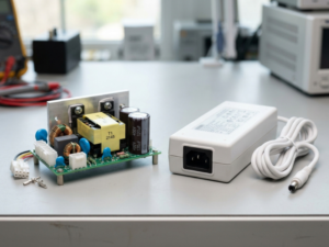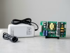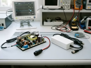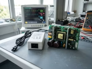
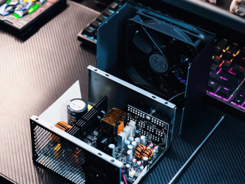
Gallium Nitride (GaN) outperforms silicon in power supplies by switching up to 10 times faster, achieving efficiencies of up to 96–98%, and enabling components 5–10 times smaller. GaN is now widely used in consumer chargers, EV systems, data centers, and industrial equipment—delivering more power in less space with significantly less heat.
Silicon has powered modern electronics for over 50 years. It’s cheap, well-understood, and backed by a massive global supply chain. But it’s also hitting a wall. As demand rises for higher-density, faster-switching power electronics—driven by AI infrastructure, electric vehicles, and compact consumer devices—silicon is running into physical limits that can’t be engineered away.
That’s where gallium nitride comes in. GaN is a wide-bandgap semiconductor that outperforms silicon on almost every electrical metric that matters in power conversion: switching speed, efficiency, heat tolerance, and physical footprint. It’s not a distant future technology. GaN-based chargers from brands like Anker, Belkin, and Lenovo are already in millions of homes. GaN transistors are being designed into EV on-board chargers, 5G base stations, and data center power supplies right now.
This post breaks down why GaN is displacing silicon in power applications, how it performs in real-world conditions, where it’s being deployed, what the implementation challenges look like, and what to watch for when selecting GaN hardware.
The Physical Advantage of GaN Over Silicon
The performance gap between GaN and silicon starts at the atomic level.
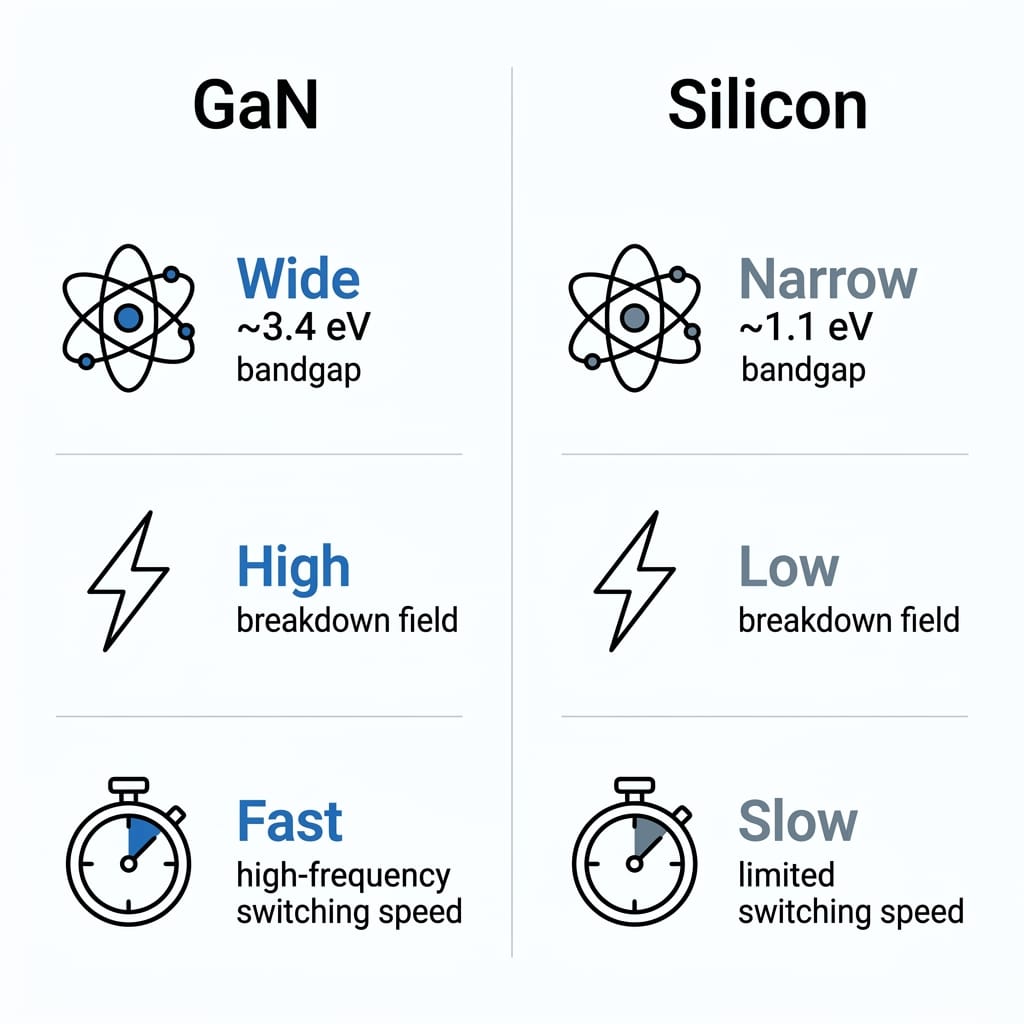
Silicon has a bandgap of 1.1 eV—the energy required to free an electron and allow conduction. GaN has a bandgap of approximately 3.4 eV, which is more than three times that of silicon. That wider bandgap is why GaN is classified as a wide-bandgap (WBG) semiconductor, and it has direct consequences for how hard you can push the material.
A wider bandgap means the material can withstand much higher electric fields before breaking down. GaN’s critical breakdown field is roughly 3.3 MV/cm, compared to 0.3 MV/cm for silicon—an 11-fold difference, according to research cited in AZoM (Abbas, 2026). This allows GaN devices to block higher voltages over much shorter distances, which directly reduces on-state resistance and energy loss during switching.
GaN also benefits from high electron mobility. In GaN-based high-electron-mobility transistors (HEMTs), electrons move through the channel at 1,500–2,000 cm²/Vs. That compares to approximately 1,450 cm²/Vs for silicon—but in practice, GaN devices switch 10 times faster than silicon MOSFETs and up to 100 times faster than IGBTs, according to EPC (Efficient Power Conversion Corporation). The reason is that higher electron mobility, combined with GaN’s smaller transistor geometry, means lower capacitance and shorter current paths.
The bottom line: GaN transistors can operate at switching frequencies of 1–10 MHz, while silicon typically tops out below 100 kHz. That frequency advantage cascades through the rest of the power supply design in ways that matter greatly to engineers.
Improving Efficiency and Reducing Energy Waste
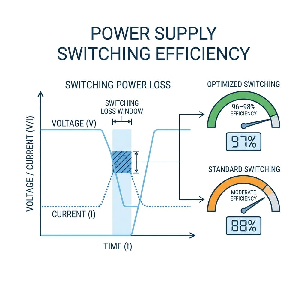
Every switching transition in a power supply creates a brief window where energy is lost. The faster a transistor switches, the shorter that window. GaN’s high switching speed translates directly into lower switching losses.
In practical terms, GaN-based power supplies achieve efficiencies of up to 96–98%, compared to 85–90% for traditional silicon designs, according to Phihong USA. A GaN-based reference design published by EPC demonstrated a 48V-to-12V power converter operating at 96.3% peak efficiency while delivering 1 kW into a 12V load—with module dimensions of just 17.5 × 22.8 × 7.7 mm.
In solar microinverters, GaN bidirectional switches enable single-stage power conversion with efficiencies exceeding 97.5% and power densities up to 40% higher than silicon equivalents (AZoM, 2026).
For data centers—which could account for up to 12% of U.S. electricity consumption by 2028—the implications are significant. A worldwide upgrade from silicon to GaN power supplies is estimated to reduce energy loss by 30–40%, saving over 100 TWh and avoiding 125 million tons of CO₂ emissions by 2030, according to Navitas Semiconductor.
Less energy lost as heat also means lower cooling requirements. GaN power supplies typically run cooler than their silicon counterparts under equivalent loads. That matters not just for efficiency but for component longevity and system reliability.
Why Small Sizes Are Possible With GaN
GaN transistors are 5–10 times smaller than equivalent silicon devices (EPC). That’s a significant reduction in die area, but the size benefit doesn’t stop at the transistor itself.
Because GaN operates at much higher switching frequencies, the passive components in a power supply—transformers, inductors, capacitors—can be made smaller. These passives store energy during each switching cycle; the higher the frequency, the less energy they need to store per cycle, and the smaller they can be. This reduction in passive component size is often what enables the dramatic shrinkage seen in GaN charger designs.
GaN-based on-board chargers (OBCs) in electric vehicles can achieve efficiency ratings of 96–98% while reducing system volume by 30–60% compared to silicon alternatives (AZoM, 2026). In mobile fast charging, GaN power ICs enable chargers that are approximately half the size and weight of silicon-based adapters while delivering the same or higher power output, according to Navitas Semiconductor.
The most visible consumer example is the compact wall charger. A GaN charger capable of delivering 65W or 100W to a laptop can fit in a form factor that traditional silicon designs couldn’t achieve at half that wattage. Anker, for instance, offers a 100W GaN charger measuring approximately 1.7 × 1.1 × 2.7 inches—smaller than most single-port silicon chargers from five years ago.
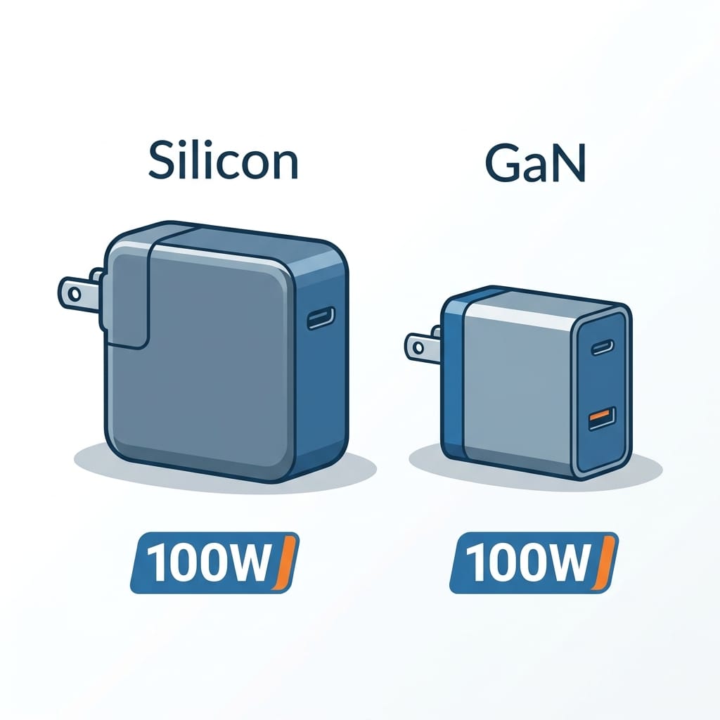
For industrial and aerospace applications, where every gram and cubic centimeter carries a cost, this size advantage has real economic and design implications. Robotics, drones, satellite systems, and medical devices all benefit from power electronics that can do more in a smaller footprint.
Practical Applications in Consumer and Industrial Tech
GaN is no longer a niche material for specialized military or RF applications. It’s entered mainstream production across several major sectors.
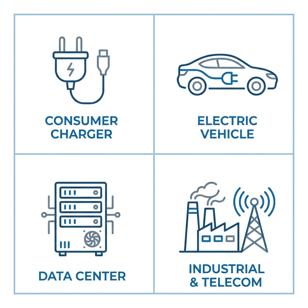
Consumer electronics represent the largest current market for GaN power ICs. Mobile fast charging is the primary driver, with GaN chargers from Dell, Lenovo, Samsung, AUKEY, Baseus, Anker, and Belkin now widely available. Navitas Semiconductor reported shipping over 18 million GaN power ICs with zero failures as of early 2021—a number that has grown significantly since.
Electric vehicles are a rapidly growing application. GaN-based OBCs and DC-DC converters improve efficiency and reduce the physical size of EV charging hardware. Research published in IEEE Transactions on Electron Devices (2026) highlights GaN gate structures with threshold voltages exceeding 4V, improving safety and reliability in automotive-grade designs.
Data centers and AI infrastructure are adopting GaN to manage the power demands of high-density compute. GaN-based power supplies reduce energy losses in server rack power delivery while enabling greater computational density per square foot—a key priority as AI workloads continue scaling.
Industrial and telecom applications include motor drives, programmable logic controllers, 5G base stations, and fiber-optic communication systems. GaN’s high-frequency switching is particularly useful in RF applications, where silicon has always struggled at higher frequencies.
Medical equipment is another growing area. Devices such as ventilators, infusion pumps, and imaging systems rely on GaN power supplies that meet IEC 60601-1 safety standards while delivering stable, low-noise power.
Common Obstacles and Implementation Costs
GaN’s advantages are real, but it’s not a drop-in replacement for silicon in every situation. There are legitimate challenges to understand before specifying GaN components.
The initial component cost remains higher than that of silicon in many product categories. GaN transistors require specialized fabrication processes, and while costs have been falling, higher-power GaN components can still represent a meaningful premium over equivalent silicon devices. That said, for lower-voltage devices under 500V, GaN transistors from manufacturers like EPC now match or undercut comparable silicon MOSFET pricing—driven by smaller die size, higher manufacturing yields, and simpler packaging requirements.
Supply chain depth is still maturing. The supplier base for high-quality GaN components is narrower than for silicon, which can create sourcing risk for OEMs scaling production. Partnering with manufacturers who have established GaN-specific supply chains reduces that risk.
Design learning curve is real but manageable. GaN enhancement-mode transistors behave similarly to silicon MOSFETs, which means engineers with MOSFET experience can adapt without starting from scratch. EPC notes that more than 100 universities worldwide now incorporate GaN into their power electronics curricula.
Thermal management in high-power GaN applications still requires careful attention. Although GaN runs cooler than silicon under equivalent conditions, high-wattage GaN designs still generate heat. PCB layout, gate drive design, and thermal interface materials all affect performance. In chip-scale GaN packages, the junction-to-case thermal resistance is typically lower than silicon—but this advantage only holds when the rest of the thermal path is properly engineered.
Regulatory compliance adds another layer. GaN power supplies must meet efficiency and safety standards, including DOE Level VI, EU CoC Tier 2, UL 62368-1, and IEC 60601-1 for medical applications. These requirements are well-established but require deliberate design effort and third-party certification.
Identifying Quality GaN Hardware
Whether you’re evaluating a GaN charger for personal use or specifying a GaN power module for a production design, several factors separate reliable hardware from underperforming or unsafe products.
Power output and wattage should match your application. For smartphones and small devices, 30–45W is typically sufficient. Laptops and multi-device charging stations generally need 65W or above. At the industrial and professional level, GaN power modules range from hundreds of watts to multiple kilowatts.
Certifications matter. Look for products compliant with UL, CE, FCC, and RoHS. For consumer chargers, DOE Level VI efficiency certification is a reliable indicator of quality. Medical-grade GaN supplies should carry IEC 60601-1 certification.
Built-in protection features are non-negotiable. Reliable GaN hardware includes overcurrent, overvoltage, and short-circuit protection, as well as active temperature monitoring. Anker’s ActiveShield technology, for example, monitors charging temperatures up to 3–6 million times per day, depending on the model.
Brand and sourcing. Consumer-facing GaN chargers from established brands (Anker, Belkin, Baseus, AUKEY) are built on GaN ICs from proven suppliers such as Navitas Semiconductor and GaN Systems. For industrial or OEM applications, working directly with component manufacturers such as EPC, Navitas, or Infineon provides greater control over specifications and supply reliability.
The number of ports and power distribution are relevant for multi-device consumer chargers. Confirm that the stated wattage reflects realistic simultaneous output—some chargers derate significantly when multiple ports are active.
The Future of Compact Power Delivery
GaN is still far from its theoretical ceiling. According to EPC, today’s GaN devices are approximately 300 times larger than they would be if manufactured at the material’s theoretical limits. That headroom suggests many generations of improvement ahead in switching speed, power density, and cost.
Several emerging developments are worth tracking. New Resonant Tunneling Transistor (RTT) architectures based on GaN are being proposed to merge high-frequency power conversion with AI logic processing on a single chip—a convergence that could reshape data center architecture. Renesas has also unveiled bidirectional 650V-class GaN switches targeting solar inverters, AI data centers, and other applications simultaneously.
For power engineers and procurement teams, the near-term picture is straightforward: GaN is no longer a premium-only option. For applications in the 100V–700V range requiring high switching speed, compact form factor, and strong efficiency, GaN is increasingly the practical default—not the experimental choice.
The transition from silicon won’t happen overnight, and silicon remains the right answer for cost-sensitive, low-frequency, low-power applications. But for anything where power density, efficiency, and size matter, GaN has already earned its place.
Frequently Asked Questions
What is the difference between GaN and silicon in power supplies?
Silicon (Si) has a bandgap of 1.1 eV, a critical breakdown field of 0.3 MV/cm, and maximum switching frequencies below 100 kHz. GaN has a bandgap of 3.4 eV, a breakdown field of approximately 3.3 MV/cm, and can switch at 1–10 MHz. In power supply terms, this means GaN transistors lose less energy during switching, operate at higher power densities, tolerate higher voltages in smaller physical footprints, and enable much more compact overall designs.
Do GaN chargers charge phones faster than regular chargers?
Yes, in most cases. GaN chargers can handle higher power outputs more efficiently than silicon-based chargers of similar size. When paired with USB-PD fast-charging protocols, a GaN charger rated at 65W or higher will charge compatible smartphones significantly faster than a standard 5W or 18W silicon adapter. According to Navitas Semiconductor, GaN chargers enable charging speeds up to three times faster than equivalent silicon designs.
Are GaN power supplies safe for long-term use?
Yes, with well-engineered products. GaN transistors have demonstrated excellent long-term reliability. EPC’s Phase 15 reliability report documents field reliability data that compares favorably to silicon MOSFET benchmarks. The lower heat output of GaN designs also reduces thermal stress on surrounding components, thereby extending overall product lifespan. Choose products with built-in protection features and recognized certifications.
Why are GaN chargers more expensive than standard ones?
GaN transistors require specialized fabrication and, in some voltage ranges, more complex packaging than silicon devices. Those costs are falling as manufacturing scales up and as GaN production techniques mature. At the consumer level, GaN charger prices have already dropped significantly—Navitas Semiconductor notes that single-output GaN chargers now retail at roughly half the price of previous best-in-class silicon models, with multi-output models up to three times cheaper in some cases.
Will a GaN charger work with older devices?
Yes. GaN chargers that include USB-A ports are fully compatible with older devices. USB-C GaN chargers that use standard USB-PD protocols communicate with connected devices to negotiate appropriate voltage and current levels—meaning they won’t overvolt devices that don’t support high-speed charging. A GaN charger will simply deliver the power level the device requests, even if that’s a standard 5W.
Does GaN help the environment?
Compared to silicon, GaN has a meaningful environmental advantage across its lifecycle. According to Navitas Semiconductor, GaN power ICs have a carbon footprint approximately 10 times lower than that of older silicon chips. GaN device manufacturing saves roughly 80% in process chemicals and energy, plus over 50% in packaging materials. Gallium itself is extracted as a by-product of aluminum smelting, giving it a low-impact extraction footprint. At the system level, wider adoption of GaN in data centers alone could avoid 125 million tons of CO₂ emissions by 2030.
Can Gallium Nitride withstand high heat?
GaN has a melting point above 1,600°C—approximately 200°C higher than silicon. In device operation, GaN integrated circuits have demonstrated thermal stability at temperatures ranging from 200°C to 400°C (SCIEPublish). GaN’s wide bandgap contributes to this thermal stability by reducing intrinsic carrier generation at elevated temperatures. In practical power applications, GaN transistors typically produce less heat than equivalent silicon devices because they convert power more efficiently—but they’re also significantly more tolerant of the heat they do generate.