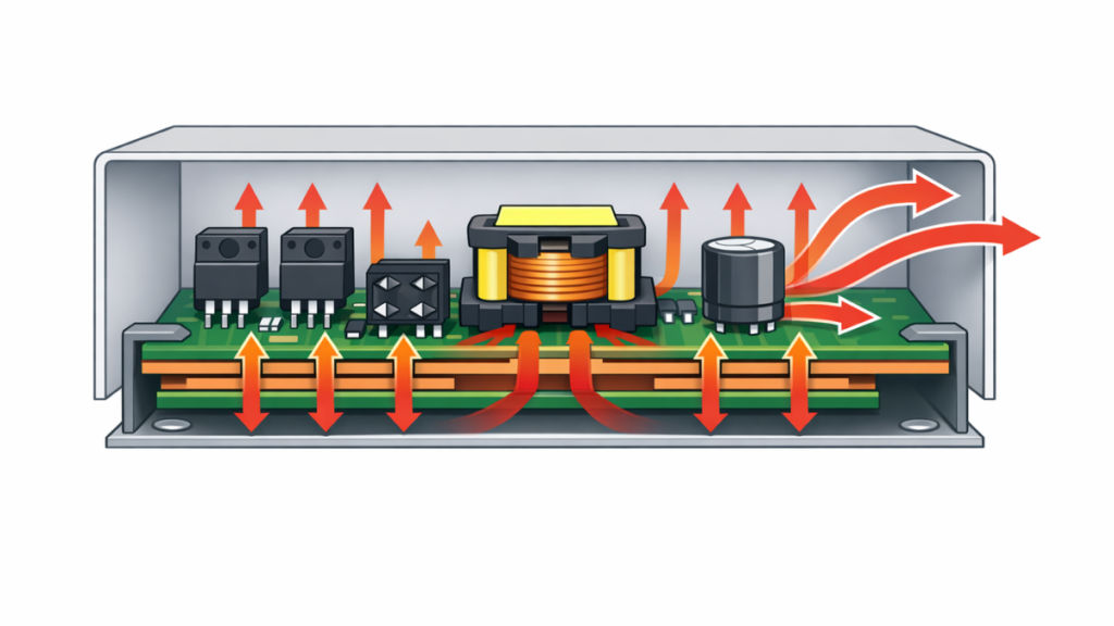
In a smaller and high-power-density AC-DC power supply, the traditional heat dissipation method will be limited. Such as the open frame power supply, wall mount power supply, and desktop power supply usually don’t use a large-sized heat sink. The internal air convection conditions are limited. In this solution, the PCB is not only an electrical connection carrier but also serves as an important part of the heat dissipation passage.
PCB in thermal design has two functions: one function is to conduct the thermal conduction by the device, and the second is to dissipate the thermal spreading over a larger area. In actual design, the PCB thermal design is often ignored; it is a correction when the temperature is over the standard. This is a basic reason for many power supply heat problems.
The basic principles of PCB heat conduction
In an AC-DC power supply, the main conduction of the device heat generated:
Component → Solder pad → Copper foil → PCB inner layer/back side → Air or enclosure
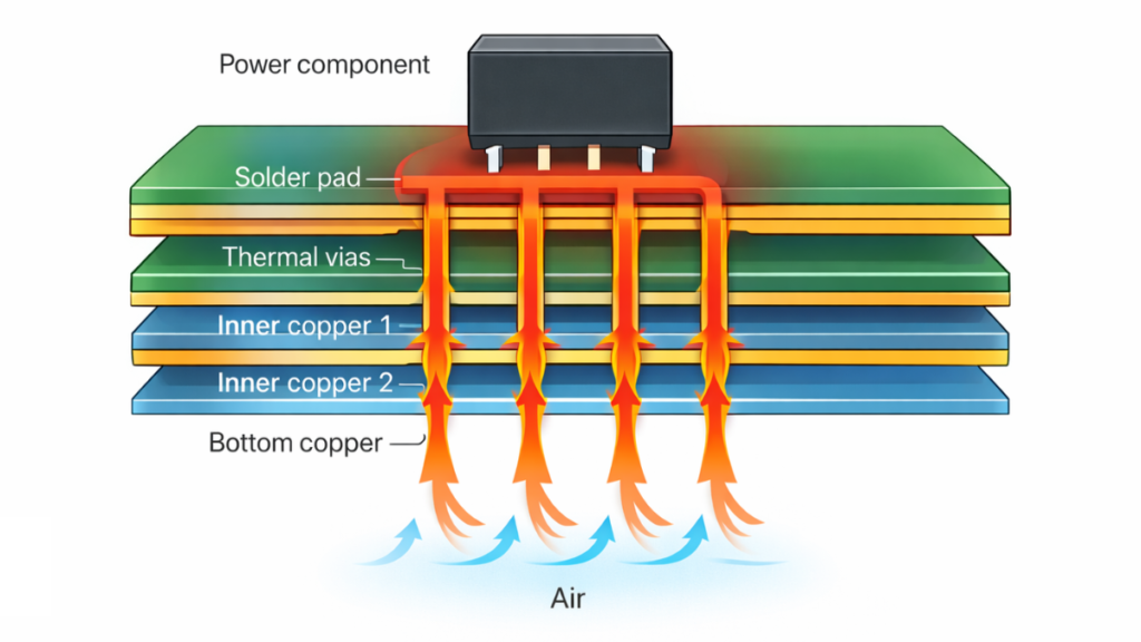
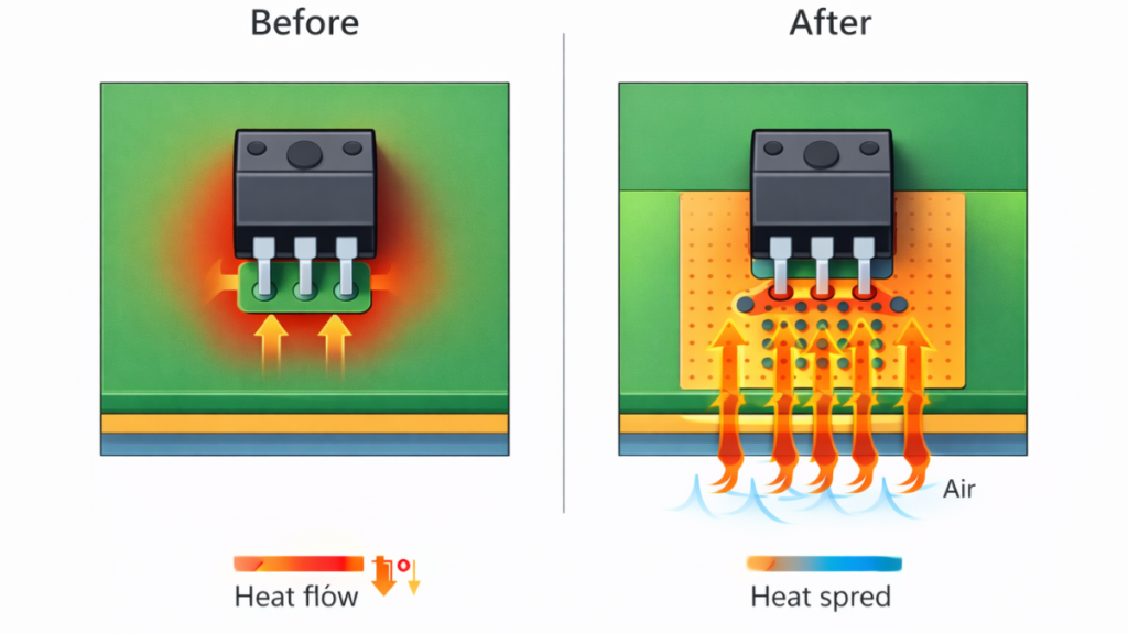
Different materials’ thermal conductivity has significant differences. The copper foil[1] has higher thermal conductivity[2] and is a thermal conductivity medium of PCB. FR-4 medium material has weak thermal conductivity. And the lower thermal conductivity performance in air. So, how to use the copper foil to conduct heat conduction and diffusion is a core issue in PCB thermal design. In engineering practice, the copper plating effectively reduces the temperature of the device. This can increase the cross-sectional area and reduce the thermal resistance, which allows heat to dissipate more quickly and evenly to other areas of the PCB.
High-heat device PCB deals with a way.
- MOSFET’s copper plating and thermal conductivity through-hole design
MOSFET power is usually a heat source in the PCB. In PCB design, you should plate enough copper sheet in the solder pads and surrounding areas. And the heat is then guided to the inner layers or the back copper foil through thermal vias so which expands the heat space. A reasonable number and distribution of vias can significantly reduce the device junction temperature.
- Heat Dissipation Layout for Rectifier Devices
Rectifier bridges and secondary rectifier devices are typically in a continuously conducting state, generating heat continuously. During PCB layout, it is important to avoid excessive concentration of these devices with other high-heat components and to provide them with continuous, low-thermal-resistance copper foil heat dissipation paths.
- Thermal Coupling Issues Between Transformers and PCBs
Although the heat distribution of magnetic devices such as transformers is relatively dispersed, their concentrated volume and limited internal heat dissipation paths require attention. In PCB design, the thermal coupling between their solder pads and copper foil should be considered to prevent long-term heat accumulation in localized areas.
Copper thickening, copper plating, and thermal vias design
- The copper thickened choice affects for temperature rise
It is efficient to reduce the thermal resistance[3] by increasing the thickness of copper. Especially shown in the high current and high heat areas. The common way includes the key to the Heat dissipation area, using 2oz or the thickest copper.
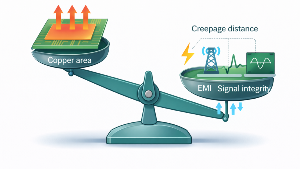
- Large volume copper plate and complete signal keep balance.
The large volume copper plate is useful for heat dissipation, and still requires the requirement of balancing creepage distance, electromagnetic compatibility, and complete signal. So, the copper plate design combined with specific circuit functions should be planned rationally, rather than increased indiscriminately.
- The number and distribution of thermal vias
The thermal vias achieve the layer heat conduction important way. Compared to a single large hole, multiple, evenly distributed small holes often provide more stable heat dissipation and have less impact on the PCB structure.
The principle of device layout and heat dissipation
The reasonable device layout is an important component in PCB thermal design. In the AC-DC power supply design process, the space of the device not only affects the electrical performance, but also decides the heat diffusion in the PCB diffusion method of PCB. If many high-heat-generating devices by layout out in the same area, it and easily lead to localized hotspots. When the device raises the temperature, and will trigger derating or failure risks. So, during the layout phase, major heat sources should be distributed as evenly as possible to avoid excessive concentration of power components.
At the same time, the high-heat-generating devices and temperature-sensitive components keep an appropriate distance. Such as electrolytic capacitors, optocouplers, etc., these are all sensitive to environmental temperature. If it is placed in a higher temperature long time, and shortens lifespan. Through reasonable isolation heat source and the sensitive device, which efficiently improves the heat layout of the whole board and system reliability.
Moreover, the device layout needs to combine the heat dissipation way for performing optimization. In natural convection conditions, the heat sources should be positioned to follow the upward flow direction of rising hot air. In applications where forced air cooling is required, that need to adjust the location of the device according to the air duct direction and let the heat diffuse easily to take off. In addition, through science, heat source dissipation and layout optimization[4] that reduce the part temperature rise and improve the whole PCB heat stability.
Common misconceptions in PCB thermal design
In engineering practice, PCB thermal design has some common misconceptions. The most common problem is that the initial design focuses more on electrical performance and letter think for the temperature factor. Even if the circuit is normal in the function test, it gradually develops a hot problem when it works for a long time or in high environmental temperatures, and increases the difficulty in post-debugging and rework.
On the other hand, the common misconception is that make power device layout concentrates on pursuing simple wiring and compact structure. This way is reasonable in electrical aspects, but easy cause the part heat to diffuse and accumulate, and the PCB appears as an obvious hot spot area. In addition, some designs just focus on the heat dissipation treatment of the PCB front, and ignore the effect of the copper sheet, inter copper plating, and integrated cooling solution for the entire board. It leads to not being useful for heat dissipation potential. These problems usually expose the sample test or long-term reliable verification phase, and effect the development cycle of product and control cost.
PCB thermal design and structure design combined
PCB thermal design is not suitable for independent conduct, and should consider the system level and overall structural design as are combined. In many AC-DC power supplies, the PCB is not only is electrical carrier but also becomes an efficient passage for heat dissipation. Such as through a reasonable PCB design, and the contact side of the shell, and the part heat diffuses to the shell, which reduces the work temperature of the device.
In addition, structural components such as fixing screws and metal brackets, while meeting mechanical strength requirements, can also participate in heat conduction as auxiliary heat dissipation paths. Only consider PCB, structural part, and shell in the thermal coupling relationship in the design stage. It can achieve a truly high-efficiency system for heat dissipation. So the PCB thermal design target is optimal single-board temperature and service to overall optimization of the entire system’s heat dissipation performance.
In all, the reasonable PCB thermal design without significantly increasing system costs efficiently reduces the work temperature in the key device and reduces external heat dissipation. Moreover, improve the long-time reliability and lifespan of the AC-DC power supply. In the background of the continued growth of high-power-density appliances, the PCB-level heat dissipation design is not only auxiliary work, but the core ability is in high-quality AC-DC power supply design.
[1]: Exploring the role of copper foil can enhance your knowledge of thermal management solutions in PCB design, leading to better performance.
[2]: Understanding thermal conductivity is crucial for effective heat management in engineering applications, especially in PCB design.
[3]: Understanding thermal resistance is crucial for optimizing heat dissipation in electronic components.
[4]: Exploring layout optimization can lead to improved thermal management and efficiency in PCB designs.