How GaN Transistor Electrical Characteristics Improve Power Adapter Efficiency And Power Density

September 27,2024
With the rapid development of electronic equipment, the market has put forward higher requirements for power adapters. High efficiency, miniaturization, and high power density have become key goals in current power adapter design. However, traditional silicon-based power devices have gradually exposed their limitations in high-frequency and high-power applications. In order to solve these problems, GaN (gallium nitride) transistors, as a new wide-bandgap semiconductor material, have become an important driving force in the upgrade of power adapter technology due to their unique electrical properties. This article will explore in detail the electrical characteristics of GaN transistors and how they can improve the efficiency and power density of power adapters.

1. Background and advantages of GaN transistors

GaN transistor is a wide bandgap semiconductor material. Compared with traditional silicon-based devices, GaN has higher electron mobility, wide bandgap and higher breakdown voltage. Due to these excellent electrical properties, GaN transistors are able to operate at higher frequencies with lower losses, significantly improving power conversion efficiency. More importantly, GaN transistors can maintain stable operation in high-voltage and high-temperature environments, making them widely used in various high-performance power supply designs.

High electron mobility

GaN transistors have an electron mobility that is about 1,000 times higher than silicon-based transistors, which means that at the same voltage, GaN devices can transmit higher density current. High electron mobility enables GaN transistors to have lower on-resistance in high-frequency switching power supplies, thereby reducing conduction losses. In a high-frequency operating environment, traditional silicon-based transistors have difficulty maintaining high-efficiency operation due to high conduction losses and switching losses. GaN transistors can effectively overcome this challenge.

High electron mobility not only improves power conversion efficiency, but also allows power adapters to operate at higher switching frequencies, thereby reducing the size of passive components such as transformers and inductors. This means that designers can reduce the overall size of the adapter while maintaining high power density to meet the needs of modern electronic devices for portability and miniaturization.

Wide bandgap and high breakdown voltage

The bandgap width of GaN transistors is approximately 3.4 eV (electron volts), compared to 1.1 eV of silicon transistors. Its wide bandgap structure allows GaN devices to withstand higher voltages while reducing leakage current. Higher breakdown voltages (typically between 600V and 1200V) give GaN devices significant advantages in high-voltage, high-power applications such as electric vehicle chargers, server power supplies and industrial-grade power converters.

The high breakdown voltage of GaN devices enables them to achieve higher power efficiency in high-power conversion applications and allows the reduction of external protection circuits in adapter designs, further simplifying circuit design and reducing system costs. In addition, GaN transistors maintain low leakage current in high-voltage applications, which also reduces system energy consumption.

Low on-resistance

The low on-resistance of GaN transistors significantly reduces conduction losses, especially during high-frequency switching operations. Compared with traditional silicon-based transistors, GaN devices have much lower on-resistance and therefore can achieve higher energy efficiency.
Influence

Low on-resistance directly improves the overall efficiency of the power adapter and reduces operating temperature. For power adapters, reducing power consumption and heat means stable operation for longer while avoiding the risk of failure due to overheating. In this way, GaN technology effectively improves the reliability of the power adapter.

2. Advantages and challenges of GaN technology in high-frequency switching power supplies


Advantages: high frequency operation

GaN transistors are capable of operating at higher frequencies than silicon-based transistors, often in the range of hundreds of kHz or even MHz. High-frequency operation allows designers to use smaller passive components such as transformers and inductors, significantly reducing the overall size and weight of the power adapter. This advantage of GaN transistors has become more prominent as the demand for small, efficient power supplies increases in markets such as portable devices, smart home products, and electric vehicles.

Size and weight advantages

Since GaN transistors can significantly increase the switching frequency, the passive components in the adapter can be significantly reduced. Compared with traditional silicon-based power adapters, adapters using GaN technology are not only smaller and lighter, but also have higher power density. This feature is very suitable for the needs of modern electronic devices for lightweight and portability, such as chargers for mobile devices such as smartphones and laptops.

Challenge: Thermal Management Issues

Although GaN transistors are more efficient, they still generate heat when operating at high frequencies. Since GaN transistors are often used in high power density designs, how to effectively manage heat dissipation becomes a design challenge. High power density means that heat is concentrated inside the adapter, and traditional passive cooling may not be enough to handle this situation. To ensure long-term device reliability, designers need to consider more efficient cooling solutions such as heat sinks, active cooling, or thermal interface materials.

Manufacturing and Cost

The manufacturing process of GaN devices is much more complex than that of silicon-based devices, which results in the current high manufacturing cost of GaN transistors. Despite its obvious performance advantages, this cost issue hinders its large-scale application in some consumer electronics fields. However, as the manufacturing process gradually matures and output increases, the cost of GaN devices is expected to drop significantly, promoting their popularization and application in more fields.

3. Practical application cases of GaN technology

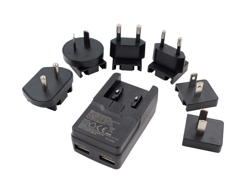
GaN technology has shown great potential in fast chargers for smartphones and laptops. By using GaN transistors, manufacturers can design charging devices that are smaller, lighter and more efficient than traditional silicon-based chargers. For example, the GaN adapter in modern smartphone fast charging technology is smaller but charges faster and more efficiently.
Data center power management

Data centers typically need to handle large amounts of power transmission, and the efficiency of power conversion is critical to overall energy consumption. GaN technology can help data center power supply equipment reduce energy consumption and improve reliability, thereby reducing operating costs and reducing environmental impact.
Electric vehicle charger

In the fast charging system of electric vehicles, GaN technology is widely used to improve charging speed and efficiency. Compared with traditional silicon-based chargers, GaN chargers are smaller and have better heat dissipation performance. They can quickly charge electric vehicle batteries while reducing the energy loss of the charging system.

4. Conclusion and future prospects

GaN transistors significantly improve the efficiency and power density of power adapters due to their high electron mobility, wide bandgap, high breakdown voltage and low on-resistance. In fields such as portable devices, electric vehicle chargers, and data center power management, GaN technology has demonstrated its excellent application prospects and huge advantages. Although GaN technology currently faces thermal management and cost control challenges, as the technology continues to mature, the cost of GaN devices will gradually decrease in the future, promoting their widespread application in more consumer and industrial products.

In the future, with further breakthroughs in GaN manufacturing technology and competition from other wide-bandgap semiconductor materials (such as silicon carbide SiC), power adapter design will enter a new era of high efficiency and high power density. GaN technology will continue to be a core force driving innovation in the power conversion field, helping the industry cope with increasingly complex power needs.

HOT TAGS
GaN
SHARE

MORE NEWS

email
hd